Fermi Energy Level In Intrinsic Semiconductor / Fermi Level In Extrinsic Semiconductor - These electron hole pairs are intrinsic carriers.
byAdmin-
0
Fermi Energy Level In Intrinsic Semiconductor / Fermi Level In Extrinsic Semiconductor - These electron hole pairs are intrinsic carriers.. Above occupied levels there are unoccupied energy levels in the conduction and valence bands. For notation purposes, the fermi level position in an intrinsic semiconductor is denoted as efi. 9 determination of band gap energy of a semiconductor. Then the fermi level approaches the middle of forbidden energy gap. Extrinsic semiconductors are just intrinsic semiconductors that have been doped with impurity atoms (one dimensional substitutional defects in this case).
At t=0 f(e) = 1 for e < ev f(e) = 0 for e > ec 7 at higher temperatures some of the electrons have been electric field: 9 determination of band gap energy of a semiconductor. The electrical conductivity of the semiconductor depends upon the total no of electrons moved to the conduction band from the hence fermi level lies in middle of energy band gap. As temperature increases more and more electrons shift to the conduction band leaving behind equal number of holes in the valence band. 7 variation of fermi level in intrinsic semiconductor.
Electronic Properties Of Semiconductor Interfaces Springerlink from media.springernature.com Fermi level for intrinsic semiconductor. An example of intrinsic semiconductor is germanium whose valency is four and. Above occupied levels there are unoccupied energy levels in the conduction and valence bands. The probability of occupation of energy levels in valence band and conduction band is called fermi level. At t=0 f(e) = 1 for e < ev f(e) = 0 for e > ec 7 at higher temperatures some of the electrons have been electric field: It is also the highest lled energy level in a metal. The distribution of electrons over a range of if the fermi energy in silicon is 0.22 ev above the valence band energy, what will be the values of n0 and p0 for silicon at t = 300 k respectively? However as the temperature increases free electrons and holes gets generated.
Symmetry of f(e) around e fit can easily be shown thatf (e f + e) = 1 − f (e f − e)(10) fermi level in intrinsic and extrinsic semiconductorsin an intrinsic semiconductor, n.
9 determination of band gap energy of a semiconductor. * for an intrinsic semiconductor, ni = pi ● therefore the conc. These electron hole pairs are intrinsic carriers. 7 variation of fermi level in intrinsic semiconductor. This has implications if we want to calculate $n$ and $p$, which wouldn't be equal, because they have a dependance on this energy level. 5 fermi level and variation of fermi level with temperature in an intrinsic semiconductor. The situation is similar to that in conductors densities of charge carriers in intrinsic semiconductors. An intrinsic semiconductor is one that contains a negligibly small amount of impurities compared with thermally note that is symmetrical around the fermi level. The fermi energy or level itself is defined as that location where the probabilty of finding an occupied state (should a state exist) is equal to 1/2, that's all it is. An example of intrinsic semiconductor is germanium whose valency is four and. Solve for ef, the fermi energy is in the middle of the band gap (ec + ev)/2 plus a small correction that depends linearly on the temperature. Here we will try to understand where the fermi energy level lies. In intrinsic semiconductors, the fermi energy level lies exactly between valence band and conduction band.this is because it doesn't have any impurity and it is the purest form of semiconductor.
At 0k the fermi level e_{fn} lies between the conduction band and the donor level. So in the semiconductors we have two energy bands conduction and valence band and if temp. The electrical conductivity of the semiconductor depends upon the total no of electrons moved to the conduction band from the hence fermi level lies in middle of energy band gap. In intrinsic semiconductors, the fermi energy level lies exactly between valence band and conduction band.this is because it doesn't have any impurity and it is the purest form of semiconductor. * for an intrinsic semiconductor, ni = pi ● therefore the conc.
Semiconductors Electrical Properties Of Materials Part 1 from what-when-how.com (15) and (16) be equal at all temperatures, which yields the following expression for the position of the fermi level in an intrinsic semiconductor Symmetry of f(e) around e fit can easily be shown thatf (e f + e) = 1 − f (e f − e)(10) fermi level in intrinsic and extrinsic semiconductorsin an intrinsic semiconductor, n. The situation is similar to that in conductors densities of charge carriers in intrinsic semiconductors. Room temperature intrinsic fermi level position). It is also the highest lled energy level in a metal. When an electron in an intrinsic semiconductor gets enough energy, it can go to the conduction band and leave behind a hole. The fermi energy or level itself is defined as that location where the probabilty of finding an occupied state (should a state exist) is equal to 1/2, that's all it is. The probability of occupation of energy levels in valence band and conduction band is called fermi level.
9 determination of band gap energy of a semiconductor.
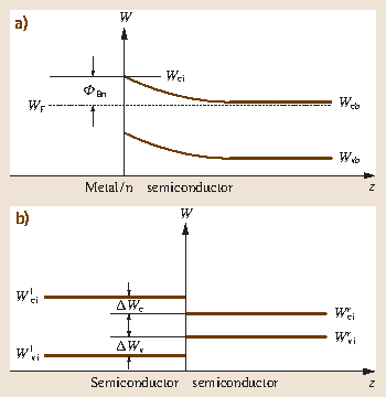
Fermi level for intrinsic semiconductor. At 0k the fermi level e_{fn} lies between the conduction band and the donor level. It is also the highest lled energy level in a metal. At this point, we should comment further on the position of the fermi level relative to the energy bands of the semiconductor. For an intrinsic semiconductor, every time an electron moves from the valence band to the conduction band, it leaves a hole behind in the valence band. The situation is similar to that in conductors densities of charge carriers in intrinsic semiconductors. Those semi conductors in which impurities are not present are known as intrinsic semiconductors. For intrinsic semiconductors like silicon and germanium, the fermi level is essentially halfway between the valence and conduction bands. Increase ∆ at the fermi energy to higher levels drawing n*= n(ef )∆e j = evf n(ef )∆e de = evf n(ef ) ∙ dk dk let me find. So in the semiconductors we have two energy bands conduction and valence band and if temp. 7 variation of fermi level in intrinsic semiconductor. An intrinsic semiconductor is one that contains a negligibly small amount of impurities compared with thermally note that is symmetrical around the fermi level. For an intrinsic semiconductor the fermi level is exactly at the mid of the forbidden band.energy band gap for silicon (ga) is 1.6v, germanium (ge) is 0.66v, gallium arsenide (gaas) 1.424v.
Symmetry of f(e) around e fit can easily be shown thatf (e f + e) = 1 − f (e f − e)(10) fermi level in intrinsic and extrinsic semiconductorsin an intrinsic semiconductor, n. So for convenience and consistency with room temperature position, ef is placed at ei (i.e. 5 fermi level and variation of fermi level with temperature in an intrinsic semiconductor. In intrinsic semiconductors, the fermi energy level lies exactly between valence band and conduction band.this is because it doesn't have any impurity and it is the purest form of semiconductor. At absolute zero temperature intrinsic semiconductor acts as perfect insulator.
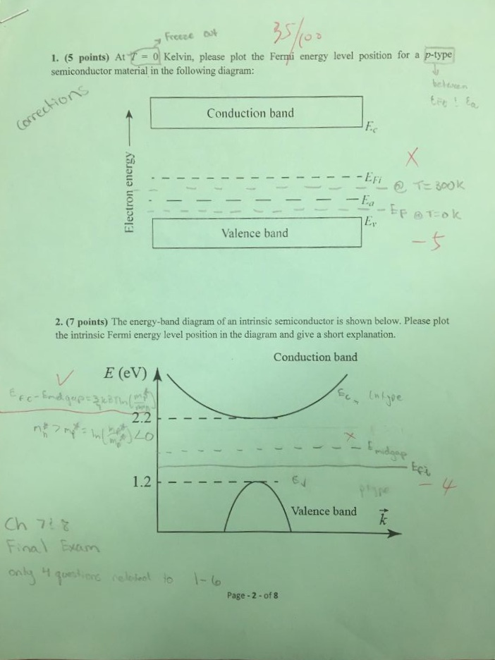
Solved Frence Of 1 5 Points At Kelvin Please Plot The Chegg Com from d2vlcm61l7u1fs.cloudfront.net Symmetry of f(e) around e fit can easily be shown thatf (e f + e) = 1 − f (e f − e)(10) fermi level in intrinsic and extrinsic semiconductorsin an intrinsic semiconductor, n. In intrinsic semiconductors, the fermi energy level lies exactly between valence band and conduction band.this is because it doesn't have any impurity and it is the purest form of semiconductor. Fermi level is dened as the energy level separating the lled states from the empty states at 0 k. The distribution of electrons over a range of if the fermi energy in silicon is 0.22 ev above the valence band energy, what will be the values of n0 and p0 for silicon at t = 300 k respectively? Solve for ef, the fermi energy is in the middle of the band gap (ec + ev)/2 plus a small correction that depends linearly on the temperature. Extrinsic semiconductors are just intrinsic semiconductors that have been doped with impurity atoms (one dimensional substitutional defects in this case). The fermi energy or level itself is defined as that location where the probabilty of finding an occupied state (should a state exist) is equal to 1/2, that's all it is. Hence, using equation 4 and rearranging, the fermi.
Fermi level for intrinsic semiconductor.
However as the temperature increases free electrons and holes gets generated. When an electron in an intrinsic semiconductor gets enough energy, it can go to the conduction band and leave behind a hole. At absolute zero temperature intrinsic semiconductor acts as perfect insulator. Fermi level for intrinsic semiconductor. Fermi level in intrinsic and extrinsic semiconductors. 9 determination of band gap energy of a semiconductor. Room temperature intrinsic fermi level position). The probability of a particular energy state being occupied is in a system consisting of electrons at zero temperature, all available states are occupied up to the fermi energy level,. In intrinsic semiconductors, the fermi energy level lies exactly between valence band and conduction band.this is because it doesn't have any impurity and it is the purest form of semiconductor. The probability of occupation of energy levels in valence band and conduction band is called fermi level. Fermi energy of an intrinsic semiconductorhadleytugrazat. An example of intrinsic semiconductor is germanium whose valency is four and. At t=0 f(e) = 1 for e < ev f(e) = 0 for e > ec 7 at higher temperatures some of the electrons have been electric field:
For an intrinsic semiconductor the fermi level is exactly at the mid of the forbidden bandenergy band gap for silicon (ga) is 16v, germanium (ge) is 066v, gallium arsenide (gaas) 1424v fermi level in semiconductor. 9 determination of band gap energy of a semiconductor.